
Automated vision inspection for defect detection plays an important role in the manufacturing sector. They are essential for detecting, quantifying, and addressing issues in a variety of electronic gadgets. Manufacturers strive for perfect quality control of all parts and completed products as technology advances. The degree of the noise of particle and crystal defects is being addressed through the development of more AOI solutions. Non-patterned wafer assessment systems and patterning wafer evaluation machines are the two broad types of wafer inspections Malaysia equipment.
The purpose and operation of the semiconductor inspection equipment or system are highlighted and discussed in this post. Highly accurate and consistent results are produced by a wafer quality inspection system, which is equipment that can detect even the smallest of faults and pinpoint their exact coordinates. Scratches, exposure issues, wafer edge faults, spin flaws, hot spots, dust contamination, and a broad variety of other defects can all harm chip performance, making regular wafer inspections crucial. It Is possible for problems to slip through final testing if they are not immediately fixed. Time and energy that could have been put into something more productive have been squandered. Product defects can shorten the useful life of a gadget.
Defects Categories
Wafer inspection machines can identify two main categories of flaws. This list includes:
- Defects in the System
The masking and exposing procedure is the root source of the defect, which means that it will be present on every projected die in the same spot on the circuit design. Locations that have difficult lighting conditions and require precise adjustment are more likely to have systematic issues. It is feasible for a typical approach of examination to overlook systematic defects in the product.
- Irregularities
This type of defect is caused by particles that become embedded on the surface of a wafer, and the locations of these particles cannot be located or predicted in advance. The primary purpose of the wafer defect inspection machine is to discover and identify faults in a wafer. This can be accomplished in several ways.
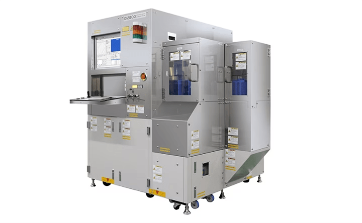
Inspection of Wafers and Sorting of Dies
Since Micro Modular System’s Die Sorter Malaysia & inspections system performs inspection before die assembly, engineers can immediately discover problems with wafer-level packages and bare dies. This is made possible by the fact that inspection takes place before die assembly. Materials such as low k components in fan-in wafer-level packages have been introduced as a result of developments in wafer-level packaging technologies. These materials are susceptible to breaking during the dicing process since they are packaged in fan-in wafer-level packages. Our solution helps chip makers decrease production risk and increase quality for mass manufacturing of increasingly complex packages in a variety of industries, including but not limited to telecommunications, consumer electronics, automotive, and more. This is accomplished by early defect detection in die sorting.
